

PL5500是一款大电流、双向四管升降压控制器 样品订购
一、产品详情
1、产品特征:
-
输入电压范围:3.5V-32V
-
输出电压范围:2.0V-30V
-
可编程开关峰值电流:20A
-
开关频率:150kHz/300kHz
-
支持1-6串充电
-
支持PWM调压、调电流
-
支持欠压保护、过压保护、过流保护、短路保护和过温保护等
-
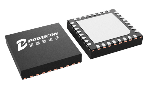
封装:QFN4x4-32
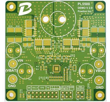
2、应用原理图:
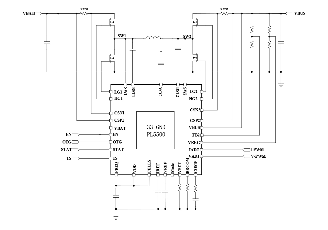
PL5500应用原理图
3、产品描述
PL5500是一款同步四开关双向降压-升压型控制器,能够调节高于或低于输入电压的输出电压。PL5500 可在 3.6 V 至 32 V(最大 36 V)的宽输入电压范围内工作,支持各种应用。PL5500可在充电器模式下为 1、2、3、4、5 和 6 节电池充电。
PL5500在降压、升压和降压-升压工作模式下采用恒定导通时间控制,可实现出色的负载和线路调节。根据 FREQ 引脚和 GND 引脚之间电阻值的不同,开关频率可设置为 150kHz、300kHz、600kHz 或 1200kHz。该器件还具有可编程软启动功能,并提供各种保护功能,包括逐周期电流限制、输入欠压锁定(UVLO)、输出过压保护(OVP)、输入过压保护、热关断和输出短路保护等。
当 OTG 为高电平时,VADJ、IADJ 引脚用于在电池放电模式下对输出 VBUS 电压和输出电流限制进行编程,这使得PL5500成为 USB 电源交付 (PD) 应用的绝佳选择。PL5500提供电压控制环、恒流环、热调节环和电池温度传感器,是电池充电管理的完美解决方案。
4、典型应用场景
-
车载电子
-
新能源供电系统
-
便携式设备
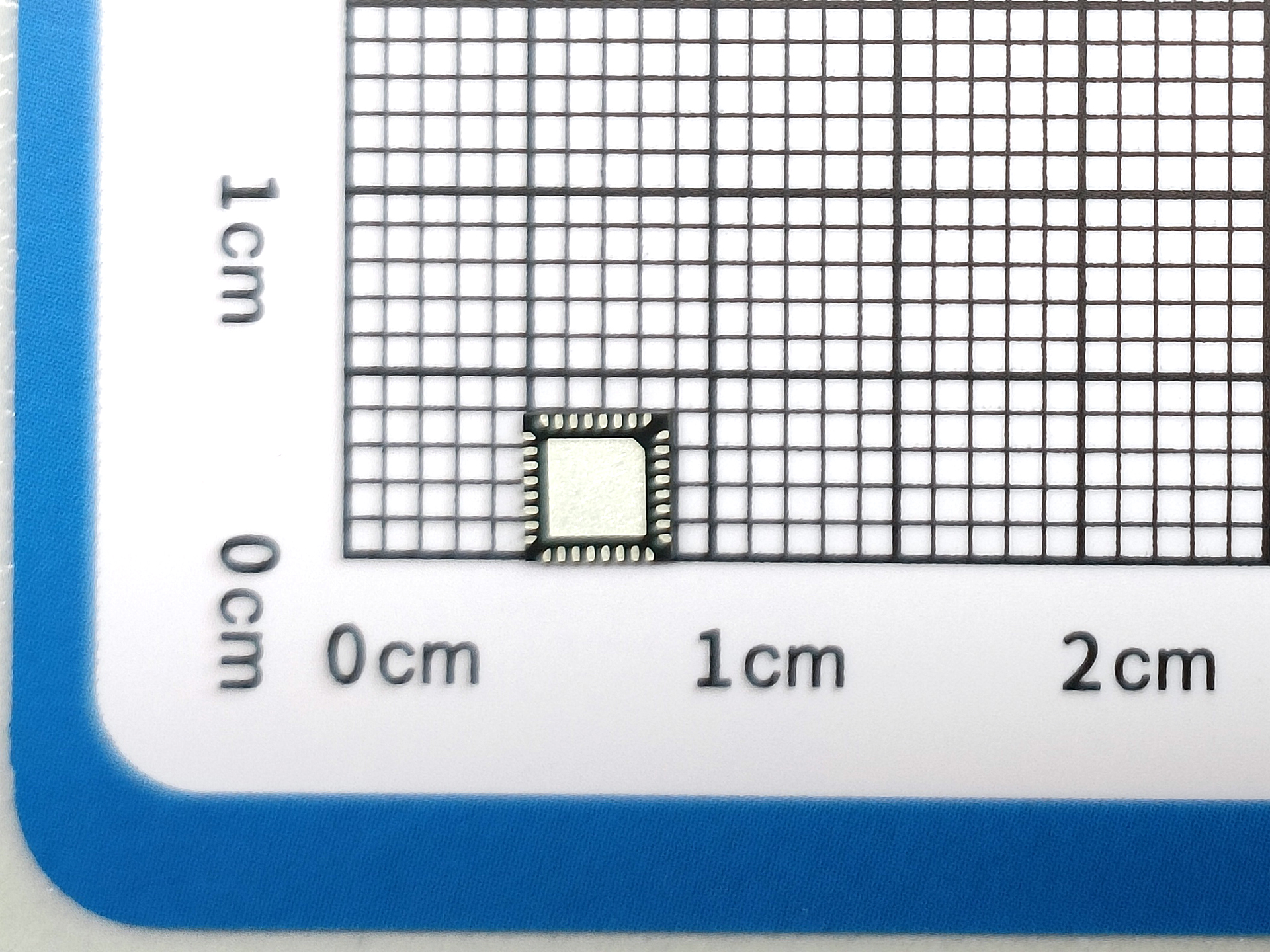
5、封装信息
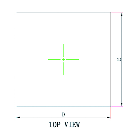
PL5500顶视图
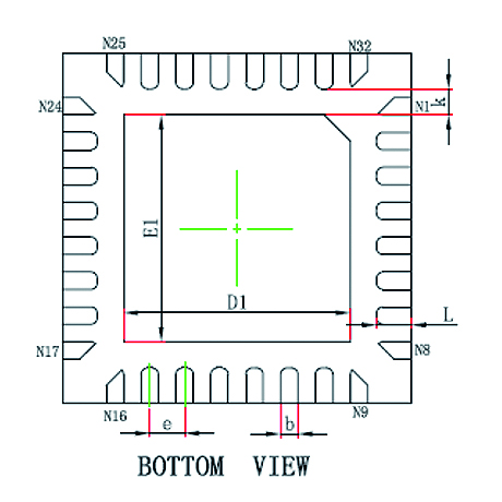
PL5500背视图
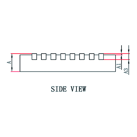
PL5500侧视图
6、管脚定义和功能描述
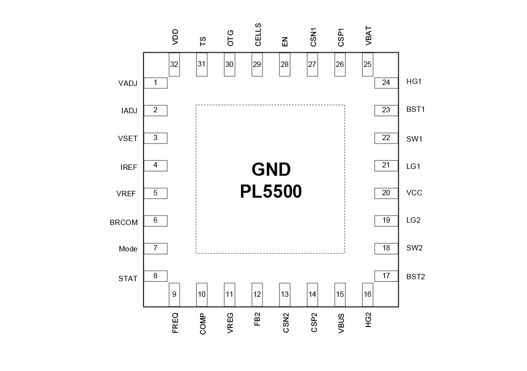
PL5500管脚定义图
管脚功能描述
| 序号 | 名称 | 描述 |
|---|---|---|
| 1 | VADJ | 连接0-2V模拟电压或PWM信号,以在VREF引脚上编程电压参考。将此引脚连接到VDD将强制VREF恒定为2V。 |
| 2 | IADJ | 连接0-2V模拟电压或PWM信号以编程IREF引脚上的电压参考。将此引脚连接到VDD将强制IREF为2V。 |
| 3 | VSET | 当OTG为低电平且PL5500工作在电池充电模式下时,在VSET和GND之间连接一个电阻器,以编程电池类型(4.2V、4.35V、4.4V、4.5V)。当OTG高于1.2V 时,VSET引脚上的电压将与CSP2和CSN2之间的电压差成正比。应用处理器可以使用此信息来监控电池放电模式下的放电电流。 |
| 4 | IREF | 输入和输出限流回路的参考电压。 |
| 5 | VREF | 电压控制回路的电压基准 |
| 6 | BRCOM | 电池内阻补偿。该引脚上的电压将与 CSP1 和 CSN1 之间的电压差成正比。应用处理器可以使用此信息来监控电池充电模式下的充电电流。 |
| 7 | MODE | CCM/DCM 模式设置引脚。Float 可以设置器件在轻载时以 DCM 模式运行,将此引脚连接到 GND 设置器件在 CCM 模式下运行。Mode 由高值电阻器在内部拉高。 |
| 8 | STAT | OTG=低时显示充电状态。当OTG=高时发出PGOOD信号。 |
| 9 | FREQ | 连接到GND以将开关频率设置为150kHz。将此引脚连接到VDD以将开关频率设置为300kHz。连接到VDD和GND之间的电阻分压器,将频率设置为600k和1200kHz。 |
| 10 | COMP | 误差放大器输出。 |
| 11 | VREG | 添加一个电阻分压器来设置VBUS调节电压。当电池充电模式下由于充电电流较大而将VBUS下拉至接近VREG设定点时,VREG调节环路将接管控制并降低下拉充电电流,以防止VBUS进一步下拉。VREG在放电模式下未激活。 |
| 12 | FB2 | VBUS电压反馈。将VBUS和GND之间的电阻分压器连接到FB2,以在电池放电模式下对VBUS电压进行编程。 |
| 13 | CSN2 | 输出电流检测的负输入。 |
| 14 | CSP2 | 输出电流检测的正输入。 |
| 15 | VBUS | VBUS 总线电压 |
| 16 | HG2 | 高侧场效应管驱动器 2。 |
| 17 | BST2 | 用于高端场效应管驱动器的升压引脚 2。 |
| 18 | SW2 | 将此引脚连接到功率级的开关点 2。 |
| 19 | LG2 | 低侧场效应管驱动器输出 2。 |
| 20 | VCC | 5.0V 电源,用于高压侧和低压侧驱动器。 |
| 21 | LG1 | 低侧场效应管驱动器输出1。 |
| 22 | SW1 | 将此引脚连接到功率级的开关管1。 |
| 23 | BST1 | 用于高侧场效应管驱动器的升压引脚1。 |
| 24 | HG1 | 高侧 MOSFET 驱动器1。 |
| 25 | VBAT | 电池电压或输入电压。 |
| 26 | CSP1 | 输入电流感应的正输入。 |
| 27 | CSN1 | 输入电流检测的负输入。 |
| 28 | EN | 高电平将启用转换器。逻辑低电平将禁用整个PL5500。EN在内部被一个高阻值电阻器拉高。 |
| 29 | CELLS | 在VDD和GND之间连接一个电阻分压器以对电池进行编程。 |
| 30 | OTG | 将OTG连接到 地(0)可以将PL5500设置为电池充电模式。连接OTG模式,将PL5500设置为电池放电模式。 |
| 31 | TS | 电池温度感应。 |
| 32 | VDD | 5.4V电源为PL5500核心电压。 |
二、技术文档
| 类型 | 标题 | 上传时间 | 文档下载 |
| 产品规格书(英文) | PL5500_Datasheet_en_ r1.1 | 2025/04/24 | PDF下载 |
三、应用方案
| 序号 | 标题 |
| 1 |
电动工具及电池包方案
电动工具及电池包方案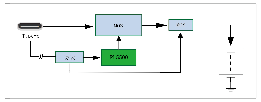
|
| 2 |
移动储能电源方案
移动储能电源方案
|


 立创商城
立创商城
 世强硬创平台